- 您现在的位置:买卖IC网 > Sheet目录473 > MAX2769EVKIT+ (Maxim Integrated)KIT EVAL FOR MAX2769
�� �
�
�MAX2769�
�Universal� GPS� Receiver�
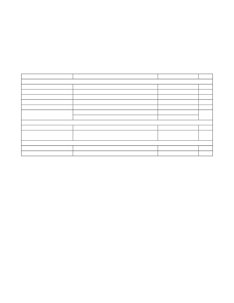
�AC� ELECTRICAL� CHARACTERISTICS� (continued)�
�(MAX2769� EV� kit,� V� CC� =� 2.7V� to� 3.3V,� T� A� =� -40� °� C� to� +85� °� C,� PGM� =� GND.� Registers� are� set� to� the� default� power-up� states.� LNA� input�
�is� driven� from� a� 50� Ω� source.� All� RF� measurements� are� done� in� the� analog� output� mode� with� ADC� bypassed.� PGA� gain� is� set� to� 51dB�
�gain� by� serial-interface� word� GAININ� =� 111010.� Maximum� IF� output� load� is� not� to� exceed� 10k� Ω� ||� 7.5pF� on� each� pin.� Typical� values�
�are� at� V� CC� =� 2.85V� and� T� A� =� +25°C,� unless� otherwise� noted.)� (Note� 1)�
�PARAMETER�
�CONDITIONS�
�MIN�
�TYP�
�MAX�
�UNITS�
�FREQUENCY� SYNTHESIZER�
�LO� Frequency� Range�
�LO� Tuning� Gain�
�0.4V� <� V� TUNE� <� 2.4V�
�1550�
�57�
�1610�
�MHz�
�MHz/V�
�Reference� Input� Frequency�
�Main� Divider� Ratio�
�Reference� Divider� Ratio�
�Charge-Pump� Current�
�ICP� =� 0�
�ICP� =� 1�
�8�
�36�
�1�
�0.5�
�1�
�44�
�32,767�
�1023�
�MHz�
�—�
�—�
�mA�
�TCXO� INPUT� BUFFER/OUTPUT� CLOCK� BUFFER�
�Reference� Input� Level�
�Sine� wave�
�0.4�
�V� P-P�
�Clock� Output� Multiply/Divide�
�Range�
�÷4�
�x2�
�—�
�ADC�
�ADC� Differential� Nonlinearity�
�ADC� Integral� Nonlinearity�
�AGC� enabled,� 3-bit� output�
�AGC� enabled,� 3-bit� output�
�±� 0.1�
�±� 0.1�
�LSB�
�LSB�
�Note� 1:� MAX2769� is� production� tested� at� T� A� =� +25� °� C.� All� min/max� specifications� are� guaranteed� by� design� and� characterization�
�from� -40°C� to� +85°C,� unless� otherwise� noted.� Default� register� settings� are� not� production� tested� or� guaranteed.� User� must�
�program� the� registers� upon� power-up.�
�Note� 2:� Default,� low-NF� mode� of� the� IC.� LNA� choice� is� gated� by� the� ANT_FLAG� signal.� In� the� normal� mode� of� operation� without� an�
�active� antenna,� LNA1� is� active.� If� an� active� antenna� is� connected� and� ANT_FLAG� switches� to� 1,� LNA1� is� automatically�
�disabled� and� LNA2� becomes� active.� PLL� is� in� an� integer-N� mode� with� f� COMP� =� f� TCXO� /� 16� =� 1.023MHz� and� I� CP� =� 0.5mA.� The�
�complex� IF� filter� is� configured� as� a� 5th-order� Butterworth� filter� with� a� center� frequency� of� 4MHz� and� bandwidth� of� 2.5MHz.� Output�
�data� is� in� a� 2-bit� sign/magnitude� format� at� CMOS� logic� levels� in� the� I� channel� only.�
�Note� 3:� The� LNA� output� connects� to� the� mixer� input� without� a� SAW� filter� between� them.�
�Note� 4:� Two� tones� are� located� at� 12MHz� and� 24MHz� offset� frequencies� from� the� GPS� center� frequency� of� 1575.42MHz�
�at� -60dBm/tone.� Passive� pole� at� the� mixer� output� is� programmed� to� be� 13MHz.�
�Note� 5:� Measured� from� the� LNA� input� to� the� LNA� output.� Two� tones� are� located� at� 12MHz� and� 24MHz� offset� frequencies� from� the�
�GPS� center� frequency� of� 1575.42MHz� at� -60dBm� per� tone.�
�4�
�Maxim� Integrated�
�发布紧急采购,3分钟左右您将得到回复。
相关PDF资料
MAX2821ETM+T
IC TXRX 802.11B 2.4GHZ 48-TQFN
MAX2829EVKIT
EVAL KIT MAX2828, MAX2829
MAX2830EVKIT+
KIT EVAL FOR MAX2830
MAX2831EVKIT+
KIT EVAL FOR MAX2831
MAX2837EVKIT+
KIT EVAL FOR MAX2837
MAX2838EVKIT+
KIT EVAL FOR MAX2838
MAX2839ASEVKIT+
KIT EVAL FOR MAX2839A WLP
MAX2839EVKIT+
KIT EVAL FOR MAX2839
相关代理商/技术参数
MAX-277
制造商:MDE 制造商全称:MDE Semiconductor, Inc. 功能描述:HIGH CURRENT TRANSIENT VOLTAGE SUPPRESSOR
MAX280C/D
功能描述:有源滤波器 RoHS:否 制造商:Maxim Integrated 通道数量:1 截止频率:150 KHz 电源电压-最大:11 V 电源电压-最小:4.74 V 最大工作温度:+ 85 C 安装风格:Through Hole 封装 / 箱体:PDIP N 封装:Tube
MAX280CPA
功能描述:有源滤波器 RoHS:否 制造商:Maxim Integrated 通道数量:1 截止频率:150 KHz 电源电压-最大:11 V 电源电压-最小:4.74 V 最大工作温度:+ 85 C 安装风格:Through Hole 封装 / 箱体:PDIP N 封装:Tube
MAX280CPA+
功能描述:有源滤波器 5th-Order Zero-Error Butterworth RoHS:否 制造商:Maxim Integrated 通道数量:1 截止频率:150 KHz 电源电压-最大:11 V 电源电压-最小:4.74 V 最大工作温度:+ 85 C 安装风格:Through Hole 封装 / 箱体:PDIP N 封装:Tube
MAX280CWE
功能描述:有源滤波器 Integrated Circuits (ICs) RoHS:否 制造商:Maxim Integrated 通道数量:1 截止频率:150 KHz 电源电压-最大:11 V 电源电压-最小:4.74 V 最大工作温度:+ 85 C 安装风格:Through Hole 封装 / 箱体:PDIP N 封装:Tube
MAX280CWE+
功能描述:有源滤波器 5th-Order Zero-Error Butterworth RoHS:否 制造商:Maxim Integrated 通道数量:1 截止频率:150 KHz 电源电压-最大:11 V 电源电压-最小:4.74 V 最大工作温度:+ 85 C 安装风格:Through Hole 封装 / 箱体:PDIP N 封装:Tube
MAX280CWE+T
功能描述:有源滤波器 5th-Order Zero-Error Butterworth RoHS:否 制造商:Maxim Integrated 通道数量:1 截止频率:150 KHz 电源电压-最大:11 V 电源电压-最小:4.74 V 最大工作温度:+ 85 C 安装风格:Through Hole 封装 / 箱体:PDIP N 封装:Tube
MAX280CWE-T
功能描述:有源滤波器 RoHS:否 制造商:Maxim Integrated 通道数量:1 截止频率:150 KHz 电源电压-最大:11 V 电源电压-最小:4.74 V 最大工作温度:+ 85 C 安装风格:Through Hole 封装 / 箱体:PDIP N 封装:Tube